Читаю вот такой фолиант Weste N., Harris D. CMOS VLSI Design_ A Circuits and Systems Perspective
https://libgen.vg/ads.php?md5=51bd9c7e9 ... 9b874dbfac1.4.3 CMOS Logic Gates
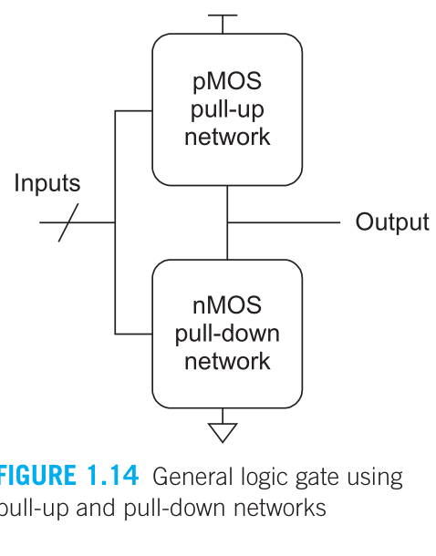
The inverter and NAND gates are examples of static CMOS logic gates, also called complementary CMOS gates. In general, a static CMOS gate has an nMOS pull-down network to connect the output to 0 (GND) and pMOS pull-up network to connect the output to 1 (VDD), as shown in Figure 1.14. The networks are arranged such that one is ON and the other OFF for any input pattern.
Это понтяно и приводится схема

In general, when we join a pull-up network to a pull-down network to form a logic gate as shown in Figure 1.14, they both will attempt to exert a logic
level at the output. The possible levels at the output are shown in Table 1.3. From this table it can be seen that the output of a CMOS logic gate can be in four states. The 1 and 0 levels have been encountered with the inverter and pull-up and pull-down networks NAND gates, where either the pull-up or pull-down is OFF and the other structure is ON. When both pull-up and pull-down are OFF, the high-impedance or floating Z output state results. This is of importance in multiplexers, memory elements, and tristate bus drivers. The crowbarred (or contention) X level exists when both pull-up and pull-down are simultaneously turned ON. Contention between the two networks results in an indeterminate output level and dissipates static power. It is usually an unwanted condition.
тоже как бы понятно и тоже приводится таблица истинности, в ссответствии с написанным гейта NAND

Читаем далее
1.4.4 The NOR Gate
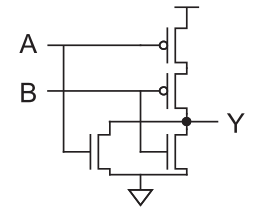
A 2-input NOR gate is shown in Figure 1.16. The nMOS transistors are in parallel to pull the output low when either input is high. The pMOS transistors are in series to pull the output high when both inputs are low, as indicated in Table 1.4.
The output is never crow-barred or left floating.
И вот собственно вопрос а почему в схеме NOR не влзникаеи кокуркеции между pull-up и pull-down частью ака верхняя и нижняя часть схемы(и соотвественно состояния Z и X не возникают), а в NAND возникают?
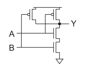
Для полноты ощущений схема NAND
